Nanotech
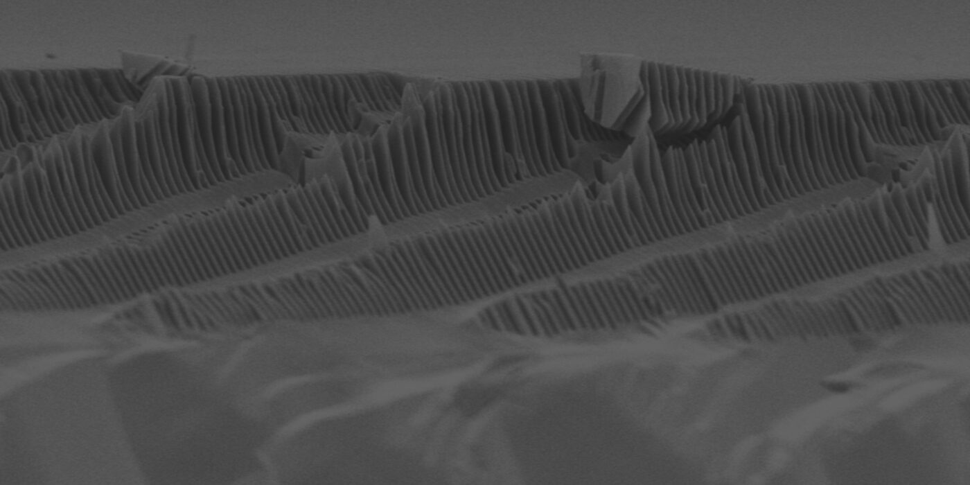
The primary mission of the Space Nanotechnology Lab (SNL) is to develop nano-fabrication, advanced lithography and precision engineering technology for building high-performance space instrumentation.
This includes x-ray telescopes and high-resolution x-ray spectrometers, magnetospheric imagers and solar physics instrumentation. SNL hardware has flown on over 10 NASA missions to date.
The SNL has a long history in developing and fabricating x-ray diffraction gratings, the key elements in x-ray spectrometers. X-ray diffraction gratings consist of extremely precise, semi-freestanding structures on the scale of tens of nanometers with extreme aspect ratios. Examples are the high energy transmission gratings on NASA’s Chandra X-ray observatory and the novel critical-angle transmission gratings under current development.
Another research focus is the improvement of grazing-incidence x-ray mirrors and mirror assemblies, which serve as the “lenses” of x-ray telescopes. The ideal format of such mirrors resembles large-area thin foils with nanometer precision shape. SNL researchers recently have pioneered several deterministic stress-based figure correction methods to improve the shape of x-ray mirrors and are currently pushing into the area of diffraction-limited x-ray optics.
Space Nanotechnology Lab is also a leader in the field of nanometer and sub-nanometer dimensional metrology applied to planar lithography patterning and ultrahigh accuracy optics. Part of this work was the development of Scanning-Beam Interference Lithography and the Nanoruler, a tool for making and measuring precise small-period gratings over square meter areas.
Education and training of students is an important part of the Space Nanotechnology Lab. Research is performed primarily by graduate and undergraduate students from the Departments of Mechanical, Electrical, Aero/Astro Engineering, and Physics with support from a small professional staff. SNL students have access to the whole range of fabrication and characterization tools available on campus, especially at MIT.nano.
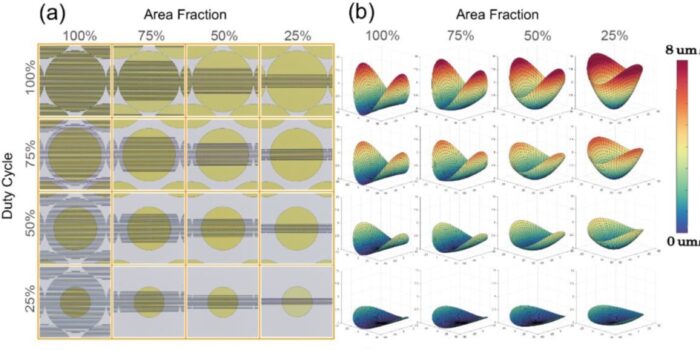
The figure errors of thin reflective optics such as x-ray mirrors can be corrected via the application of mesostructured patterns in a stressed thin silicon oxide layer on the optic backside. (a) Microscope images of the unit cell regions used for stress-based figure correction on the backsides of 16 wafers as a function of the size of stressed areas (duty cycle) and area fraction covered by anisotropic stress relief patterns (area fraction). (b) Measured deformations of silicon wafers generated by the patterns in (a). (Y. Yao et al., Optica 9, 438-444 (2022))
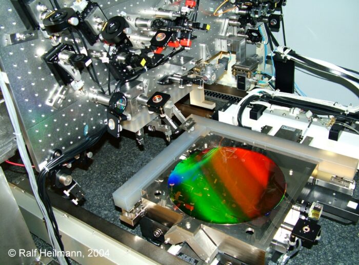
The MIT Nanoruler, a tool for the rapid high-precision patterning of gratings on large substrates (300 mm wafer shown) using Scanning-Beam Interference Lithography, developed at the SNL. (R. K. Heilmann et al., Nanotechnology 15, S504 (2004))
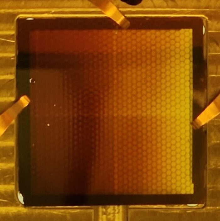
Picture of a 32x32.5 mm2 critical-angle transmission (CAT) grating, mounted in a synchrotron test plate.
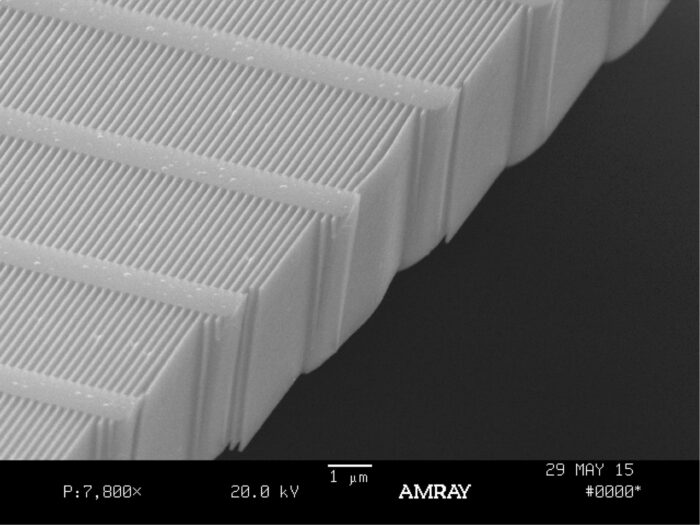
Scanning electron microscope image of a cleaved, freestanding CAT grating membrane, etched out of silicon. The fine grating bars have a period of 200 nm and a height of 4 micrometers, while the bulky integrated cross supports have a period of 5 micrometers.
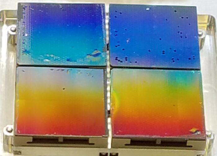
Photo of a 2x2 CAT grating “window”, a prototype grating array used in the demonstration of a spectrometer with x-ray resolving power in excess of 10,000. (R. K. Heilmann et al., Ap. J. 934, 171 1-15 (2022))